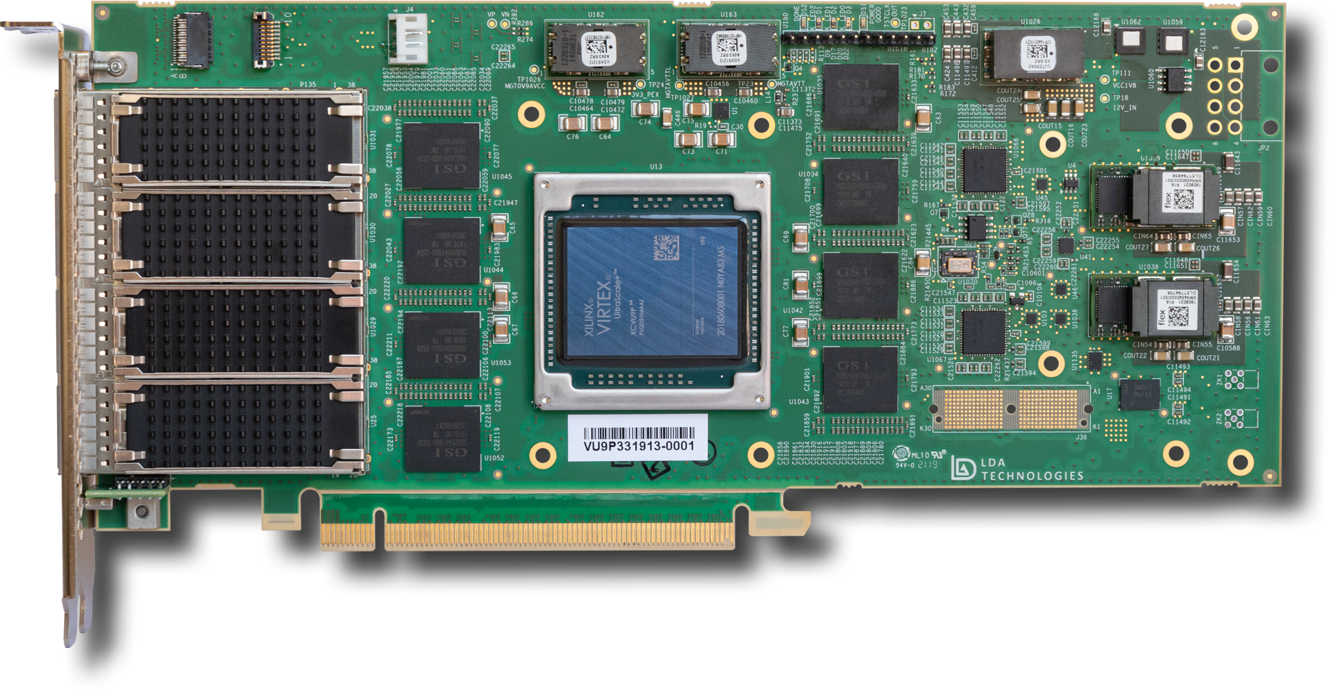
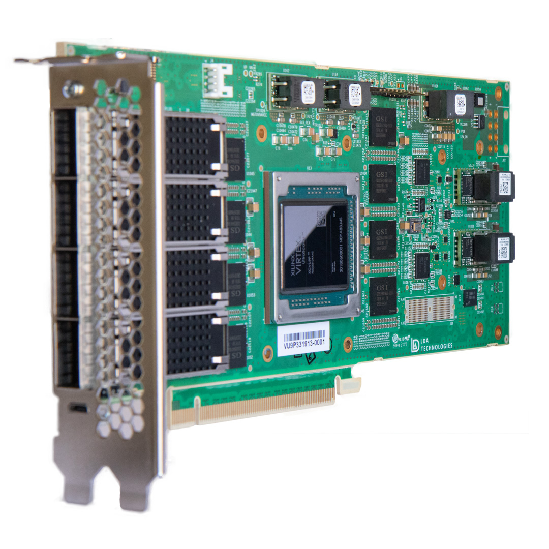
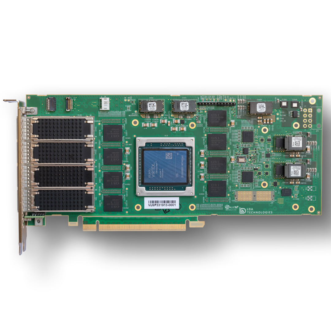
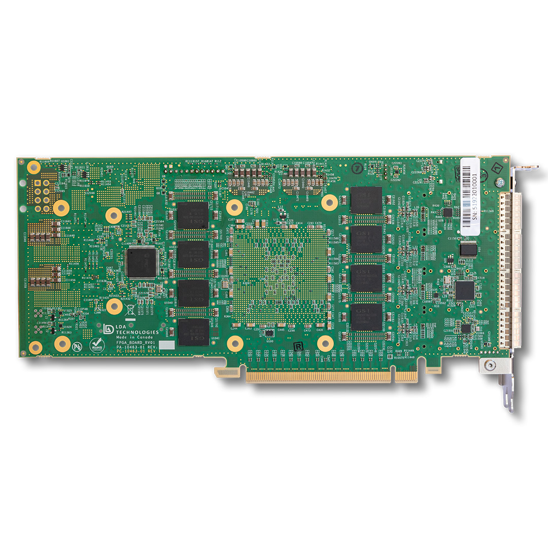
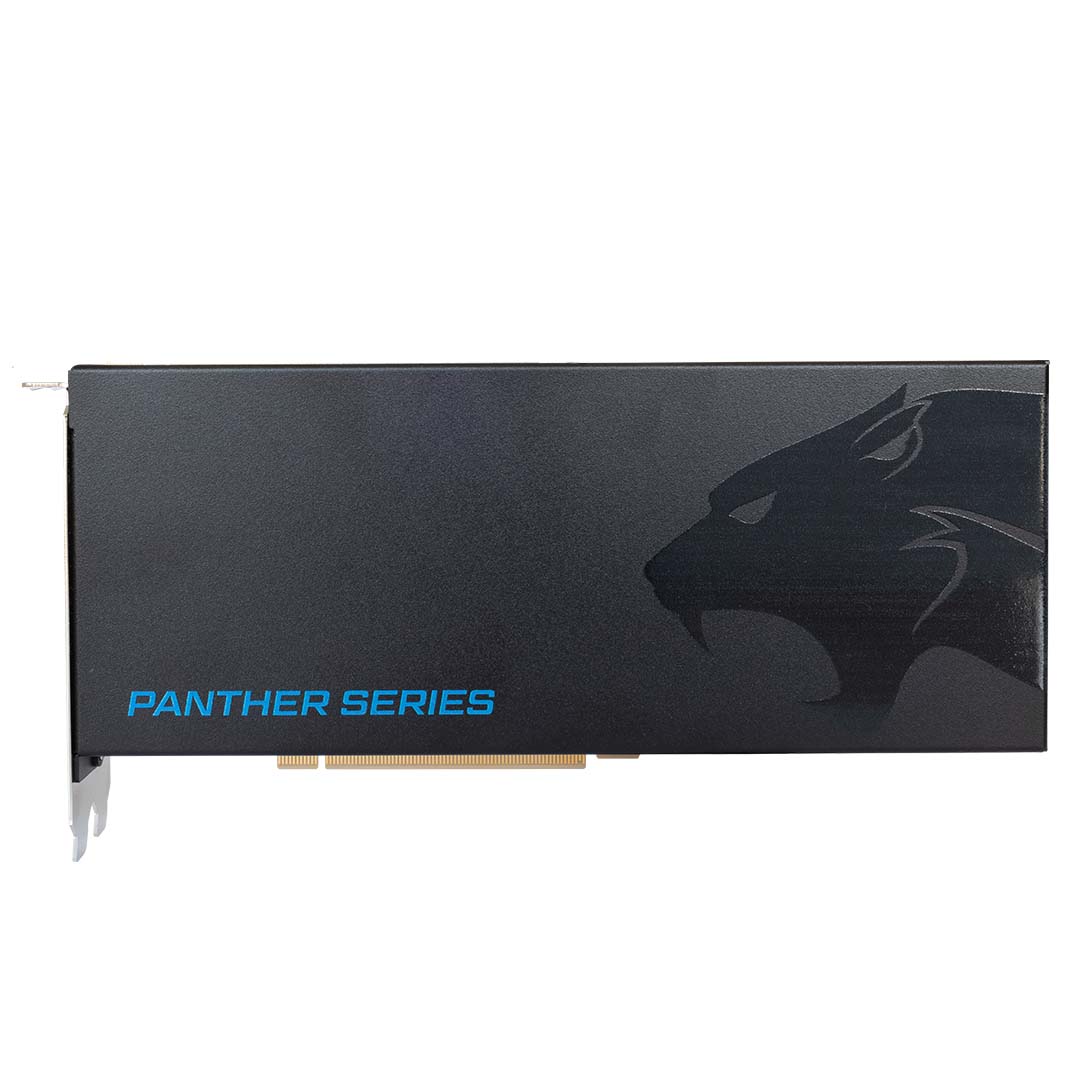
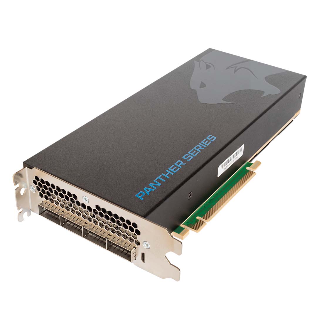
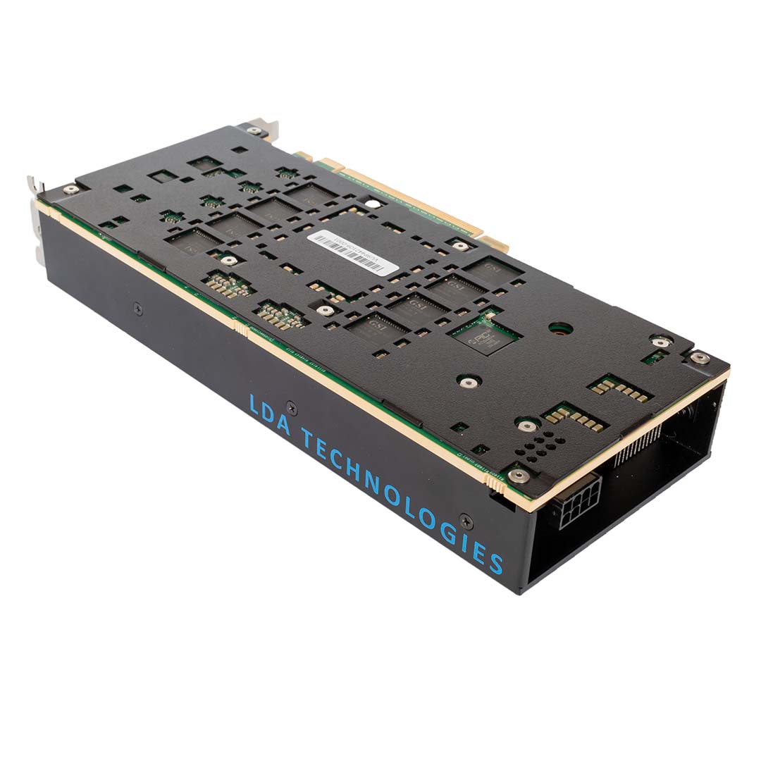
Optimize latency with jitter attenuators and ultra-low latency SyncBurst® memory: 576 MB SRAMs with a total access time of 9 ns write and 12 ns read.
Current day FPGAs handle the HFT challenge of lowest-latency tick-to-trade like no other; however, the on-chip memory available in FPGAs is not enough to cover all memory-related scenarios. So, getting the fastest memory outside the FPGA is one of the crucial points in building a successful trading system. But is it really the speed that is crucial? Does fastest equate to lowest latency? Not necessarily.
The fastest and highest bandwidth memory type most commonly available on FPGA boards today is QDR®-II SRAM. However, due to its clock specifics, accessing it from the FPGA in a typical HFT setup entails "clock domain crossing" which takes about 3 clock cycles. To put it into numbers: if the FPGA code runs at 322 Mhz then every time it accesses the QDR memory, the system pays a 9.3 ns toll. SyncBurst SRAM, on the other hand, can operate at the FPGA's local clock speed, which means clock domain crossing can be dropped along with its induced latency.
Further latency optimization is possible on this board by utilizing two jitter attenuators. This design allows the elimination of clock domain crossing between incoming and outgoing FPGA logic and locking the FPGA transmit clock to the exchange receive clock. And it can be done for two exchange feeds simultaneously.
